June 2023
Successful products are those that have precisely identified the market’s demands in terms of concept while also correctly implementing the right product architecture. The principle of "doing the right thing correctly" is also valid with regard to a product’s electromagnetic compatibility (EMC). Besides qualified engineers who develop methodical solutions, this also requires an appropriate measurement environment. At the same time, electromagnetic compatibility at the device level is so complex that only specific measurements provide meaningful results. Helbling has brought both competencies in-house for efficient and agile product development. This enables Helbling to achieve the optimum relationship between cost and quality for its clients on the basis of their inputs. This applies equally to the product and development activities.
Designing the electronics for a device has become more complex over the past five years. Whether lifestyle or medtech products, the current narrative is "sense and simplicity". Every device should be easy to use but also "smart". Paradoxically, however, this has given future generations of devices significantly more secondary functions. Touch displays, apps, Bluetooth, and AI are now required instead of buttons, switches, or levers. In addition, there is a social consensus that devices should consume less energy while in operation and be produced in a way that saves resources.
This creates a need to optimize electronic circuits at the limits of what is technically sensible and feasible. Current circuit architectures usually feature at least one of the following elements:
- Microprocessor
- Communication module
- Display
- Clocked switching stages and power stages such as the power supply unit
All elements are switched with a basic clock. An undesirable side effect of the clocked circuit topology is that there are steep flanks that emit electromagnetic interference. The interference level is usually higher than that of an analog topology. The communication module usually contains an antenna that is intended to radiate electromagnetic signals at a defined level.
A current trend is to reduce voltage levels continuously in order to consume less energy. However, this also makes the circuits more noise-prone and sensitive. Therefore, it is important to measure the interference emission emitted by the device as well as to test the interference immunity of the circuits installed in the device against radiated interference voltages.
The interrelationships in EMC are usually complex. Therefore, a decisive factor for success is to break down complexity to a manageable level. Simulations, basic theoretical knowledge, and experience help to better understand and influence certain phenomena. A simulation is only as meaningful as the model on which it is based. Components and simple assemblies can be accurately modeled and simulated with reasonable effort. At the device level, on the other hand, simulations are very costly and only inaccurately represent reality. So far, there is no "digital twin" of a device that physically reproduces the electromagnetic properties of the original with sufficient accuracy.
Only measurement can provide reliable information about device robustness regarding interference and radiation intensity. Therefore, EMC should be an integral part of product development.
EMC test capabilities in the development environment bring decisive advantages
The special, expensive EMC measurement environment and costly and complex measurement tasks are challenges that should not be underestimated. If in-house resources are not available, measurements during development often have to be carried out at accredited, cost-intensive measurement laboratories. However, experience shows that these are not geared to the dynamic environment of product development.
Helbling offers its clients heuristic development with interdisciplinary teams. The infrastructure at Helbling is adapted to the needs of development teams. They can perform all relevant EMC tests for devices in the consumer, medical, and industrial sectors on site. These are pre-compliance measurements, but they are carried out promptly and quickly during development. At the end of a development, verification of compliance with standards is formally confirmed by an accredited measurement laboratory. Among other things, this can shorten the innovation cycle.
Numerous series products with an annual production of 10k to several million units have already been launched on the market via this approach with national as well as international customers. As a rule, the entire product life cycle is managed after the start of series production. To this end, Helbling works with various OEMs around the world.
EMC Infrastructure@Helbling in detail
EMC measurements can be divided into the categories of "conducted" and "radiated" (through the air).
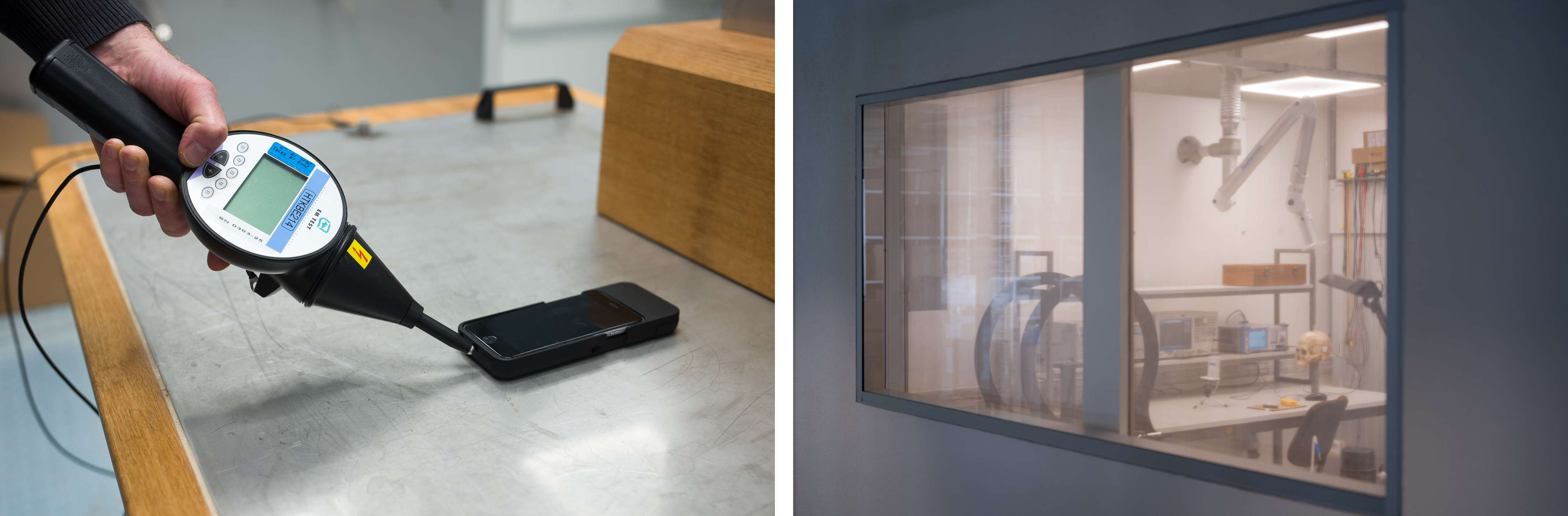
For conducted measurements, the interference levels are coupled or decoupled to the wires and conductive elements of a machine. The measurement itself is performed in a shielded room. This special room is essential so that only the device under test is measured and not external sources of interference. Additionally, the environment should not be disturbed during the immunity test.
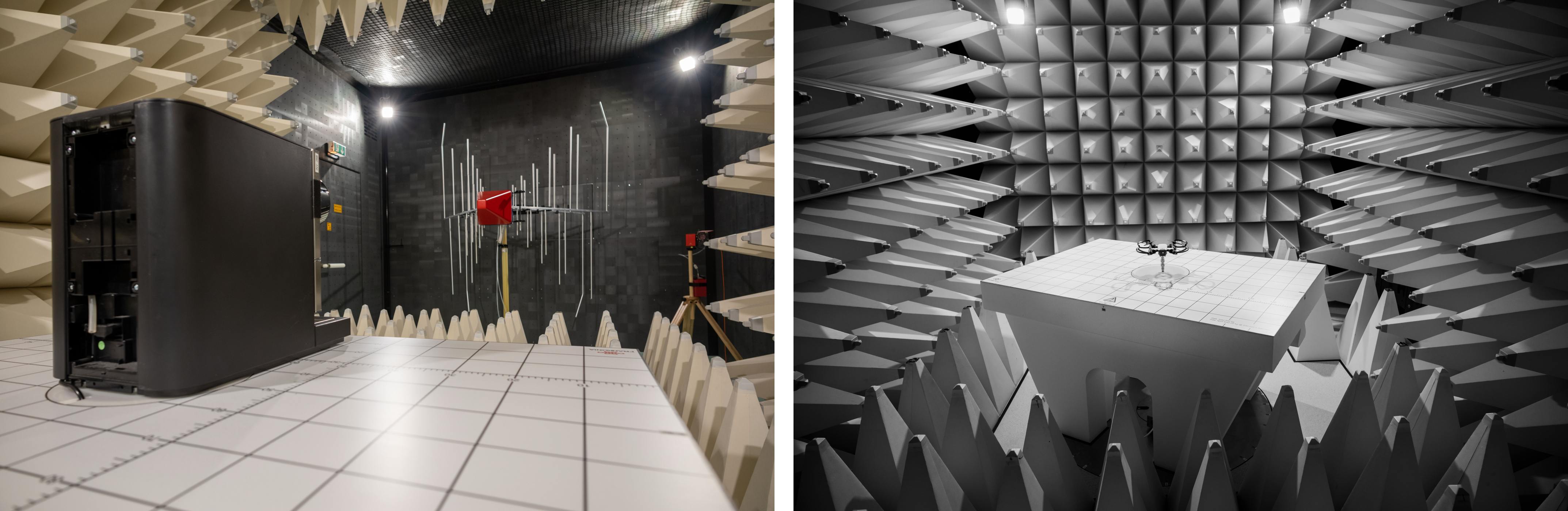
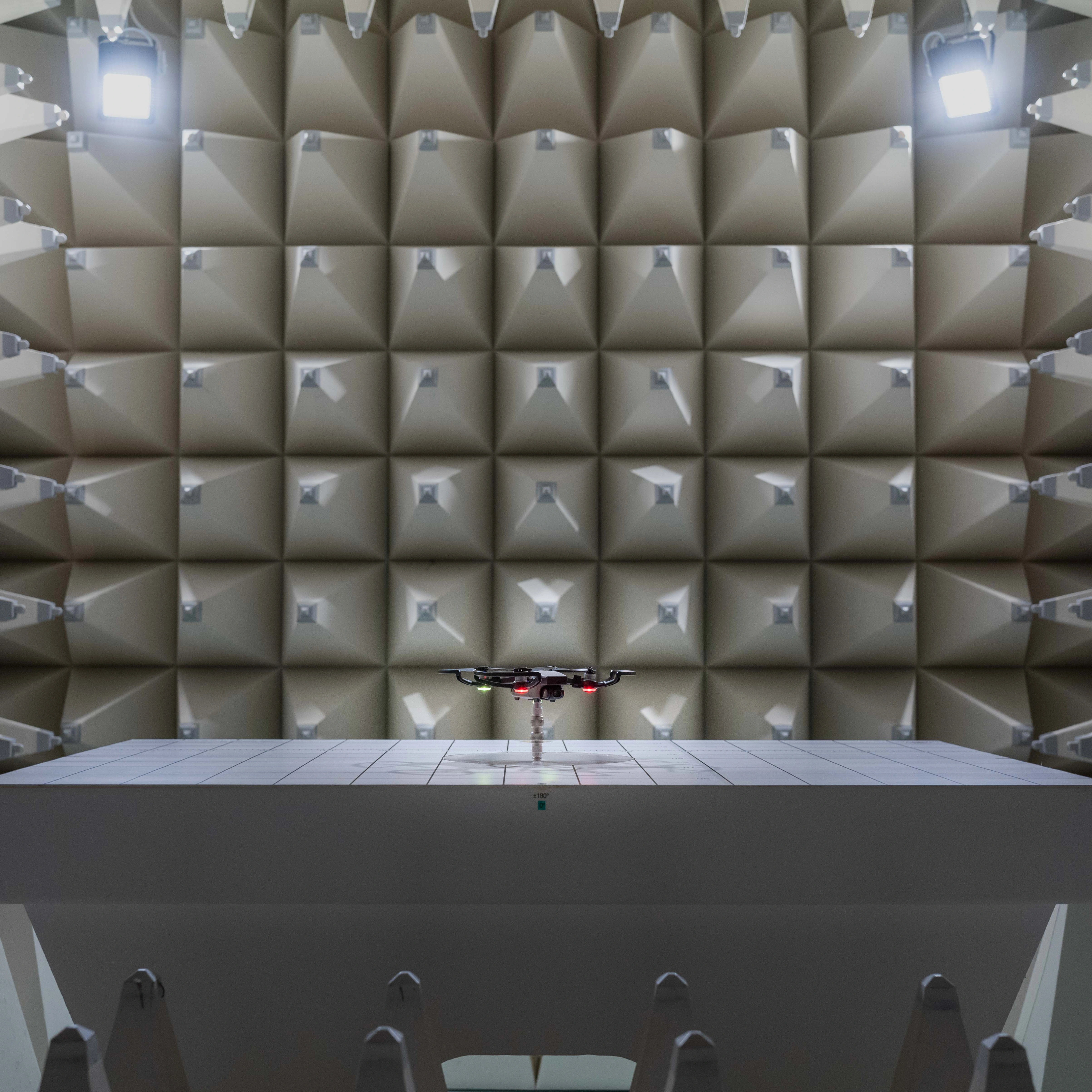
Radiated measurements are used to investigate disturbances that are transmitted through the air. An anechoic chamber is required for this purpose. An anechoic chamber is a shielded room additionally equipped with ferrite tiles and absorber cones. The surface cladding prevents uncontrolled propagation of waves by reflection.
Case study: EMC testing enables rapid response to supply chain issues
Helbling manages product life cycle management for various devices together with clients. During the coronavirus pandemic, solutions and alternatives had to be sought for components and assemblies that were no longer available due to supply constraints.
A particular challenge was to avoid production shutdowns. Many electronic components were no longer available without notice as they had been before. When it came to evaluating and approving alternative components, a solution had to be found very quickly. For the consumer goods industry in particular, it is essential to act promptly on the market. An extension to the delivery time usually reduces profit as end customers look for alternatives.
Helbling was able to adapt to the new situation immediately and offer solutions; alternative components and assemblies were immediately verified at a machine level. This also included EMC tests.
In the case study, an alternative display had to be procured for a professional beverage preparation device. The choice of displays appears large at first glance, but is reduced by specifications such as dimensions, resolution, visual impression, and touch options. Experience has shown that electromagnetic radiation from the display is a significant part of the machine’s interference level and thus makes it a critical component.
The detailed case study below describes the effects of changing a component. The interference level of the alternative display was so high that an interference suppression solution had to be developed. The methodical approach made it possible to achieve a large effect with little effort and to lower noise levels considerably.
Summary: Precise EMC measurements on site create solutions in the shortest possible time
A measurement environment for EMC tests at device level is critical for product development. This is because only specific measurements provide meaningful results in terms of device robustness with regard to interference and radiation intensity. Helbling's development teams can rely on a complete in-house EMC measurement infrastructure for projects. They have access to a shielded room for conducted measurements and an anechoic chamber for radiated measurements. This drives forward new product developments and means that optimizations can also be carried out quickly as part of the life cycle of a device.
Author: Björn Sauer
Main image: Helbling
The case study in detail
Description of measurement for display replacement
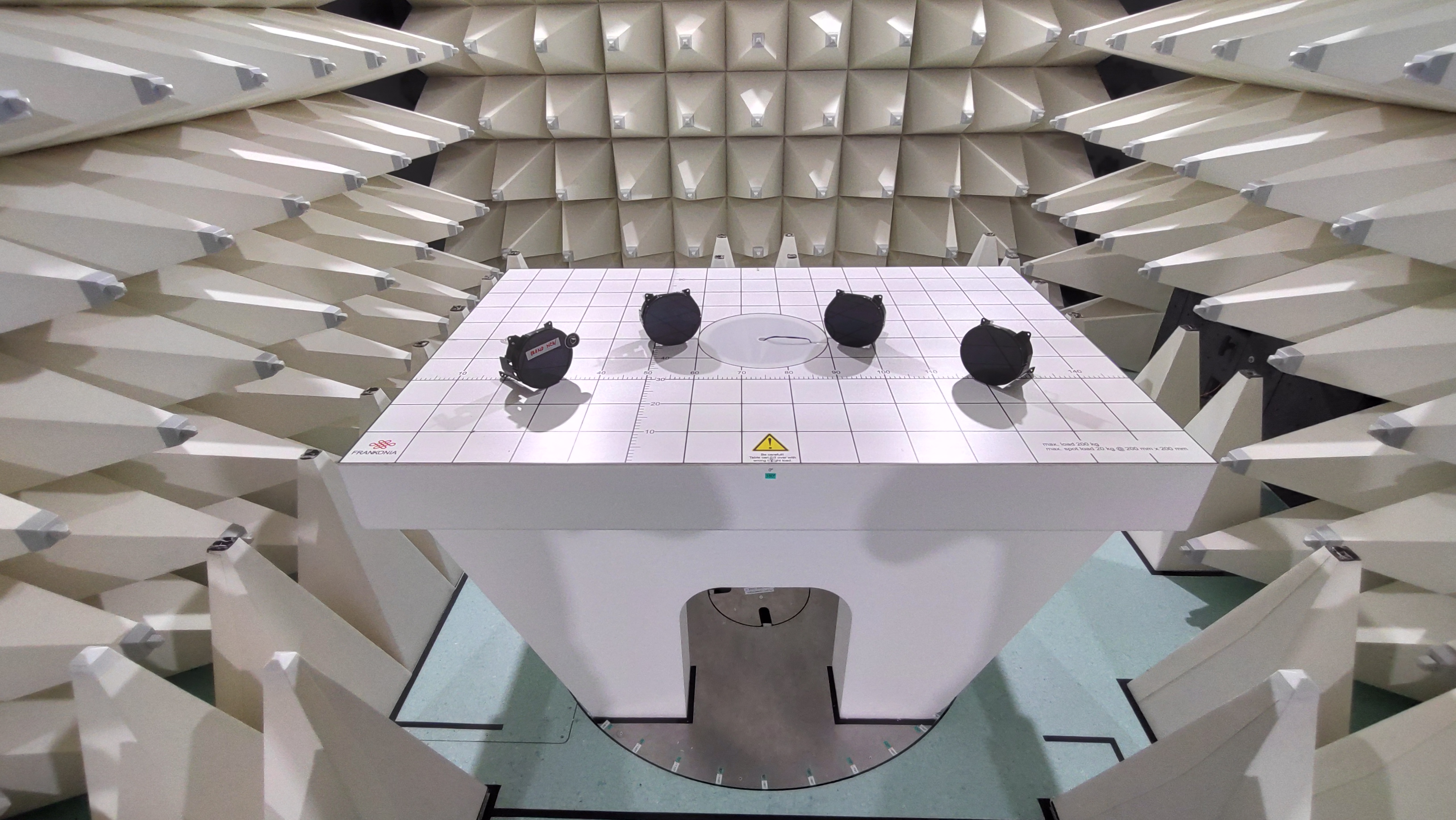
The frequencies ranging from 30 MHz to 1 GHz and 6 GHz respectively are relevant for the radiated electromagnetic compatibility of consumer, business-to-business, medical, and industrial equipment. Measurement of the electromagnetic interference radiated by the machine takes place in the anechoic chamber. Recessed in the floor of the anechoic chamber, there is a turntable on which a table is placed. The display is aligned on the turntable and put into operation. An antenna receives the interfering signal and a measuring receiver evaluates the received signal. After a frequency sweep is completed, the table is rotated and a new measurement is started. This shows the radiation all around the display, i.e. through 360 degrees.
The initial situation for the case study was that three displays were pre-selected commercially and on the basis of technical data. These displays were measured in the anechoic chamber. It was noticeable that all three displays had a pronounced peak at 300 MHz. This peak can be seen in the figure below. Display A and C have a higher peak than B, so B was selected.

Behavior of the alternative display in the machine
The next question was:, "How does the display behave in the machine housing?" Display B was installed in the machine and the measurement was repeated. The figure 5 below shows the change when the display is installed in a machine. The peak at 300 MHz has decreased, but a new peak has been added at 500 MHz, which is too close to the limit. The 500 MHz peak clearly shows how the radiation behavior of an assembly can change when installed. This peak could not have been predicted from individual measurement of the displays alone.

It is now interesting for the developer to understand what happened at 500 MHz. For this purpose, a different representation is chosen. Figure 6 shows the field strength of the individual position directions as a function of the angle. The left diagram visualizes the measurement of the display as a single component and the right diagram visualizes the measurement with the display built into the machine. It is possible to see how the polarization changes and the electrical field is radiated in the direction of the machine front. The machine and its housing act as reflectors for this electromagnetic wave.

This measurement at machine level identified the risk of being close to the normative limit, which could lead to non-standard conformity in a subsequent external measurement. After consultation with the customer, it the decision was made to optimize the display to have more margin.
Optimization
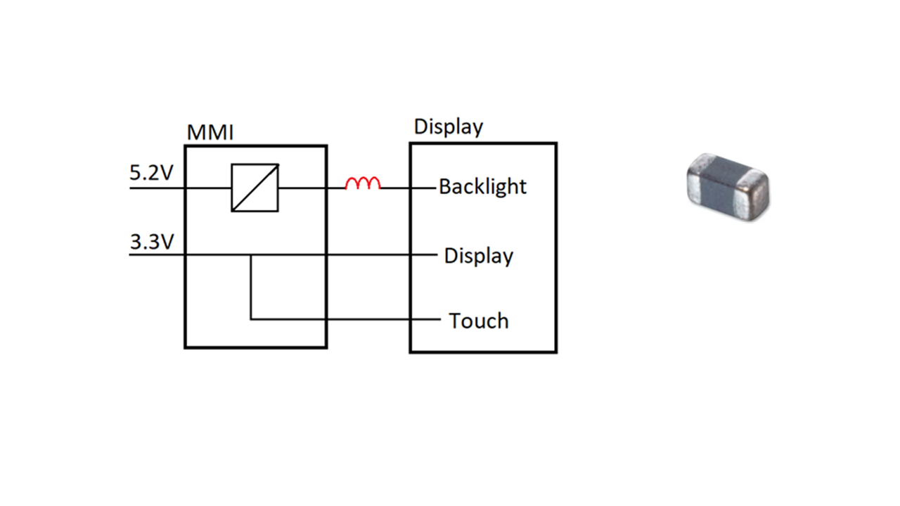
Further measurements were carried out with the display built into the machine for optimization. The functional units of the display were switched on successively in order to determine their interference level. Figure 7 shows the interference level of the controller in pink. In addition to this level, the display is shown in yellow and the backlight in blue. To the right of the peak, the amounts of individual interference levels are shown graphically. The display itself has the highest level, followed by the controller. The backlight makes up a lower proportion.

In terms of their circuitry, the display and controller are closed units. Modifying these units is very complex. The circuitry of the backlight, on the other hand, is much simpler and has potential for improvement that has not yet been exhausted. For this reason, the circuitry of the backlight was analyzed and possible optimizations were worked out (see Figure 8). A short simulation made it possible to selectively choose a ferrite. Ferrite beads are a very small and inexpensive component in the single-digit euro cent range. A significant effect was achieved with minimal additional effort.
Finally, another measurement was performed as verification: The high peaks at 300 MHz and 500 MHz could be reduced to such an extent that there was sufficient reserve to the limit and there was no longer any risk of not passing a normative approval measurement at an accredited measurement laboratory.